Last week I had the privilege and joy of traveling to Mountain View for Google’s inaugural Project Ara developer’s conference. Roberto Baldwin of The Next Web interviewed me and a couple others about our thoughts, and below I want to talk about the conference and expand on what I meant in the interview.
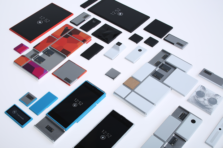
If you’re not familiar with Project Ara, here’s the quick run down: Google wants to do for smartphone hardware what “apps” and “app stores” have done for smartphone software. The crux of the idea is to create an endoskeleton, or endo, which is a frame that hardware developers can create modules for. These modules slide in from the sides and are held in place by two small electro-permanent magnets, or EPMs. The interesting thing about EPMs is that they can have their effective magnetic strength modulated. Modules are held tightly to the phone when they are in use, but easy to remove when so desired. It is intended to be an extremely flexible system, with support for multiple batteries, chargers, cameras, and just about everything else you could imagine a phone having.
It’s one thing to have a good idea, but porting the app model to hardware is easier said than done. Hardware will always have bigger barriers to creation than software. It’s a consequence of being tangible! With that in mind, Metamorph Software is developing a (free, open?) toolkit called Metamorphosys intended to be the one stop shop for simulation and analysis of modules pre-manufacture. It plugs right into other companies’ thermal sim, SPICE sim, and CAD software. They gave a very early demo of it at the conference which has me quite worried. A system under test is described by creating graphical nodes which represent different parts and subsystems and wiring them together to represent their relationships. Unfortunately, the early version looked pretty clunky due to, among other things, a (very) busy UI and unnecessarily huge icons. It was definitely nothing like, say, LabVIEW, which I think of as the gold standard for good graphical system design. I’m hoping there are some serious GUI overhauls, but again, this was an early version, so it’s unfair to form a real opinion quite yet.
When I read through the Module Developer’s Kit (MDK), a few requirements for the modules had me a bit concerned that production of these modules wouldn’t be quite as accessible for small developers as Google would like it to be. What really jumped out to me is the fact that these modules communicate with the endo through capacitive coupling. This means that every module needs to be manufactured with 8 big filled vias right on the board! Now, I can design a PCB and get a prototype produced relatively quickly for about $30, but that means abiding by a strict set of manufacturing guidelines. My PCB will get made on a big panel with other customers’ who also followed the same manufacturing guidelines, and because our boards are designed a similar way, they can be manufactured at the same time and save everyone money. However, this standard manufacturing flow does not include filled vias — for hobbyists these are pretty unusual! My board would need it’s own panel. The same module that would cost me about $30 to make could now cost upwards of $200! (and probably more) That’s a substantially higher barrier than it needs to be. In the interview, I mentioned that I thought Google (or a smart PCB manufacturer) should organize panels using the standard “Project Ara manufacturing spec.” which includes black solder mask and filled vias. If module developers could split manufacturing costs of PCBs like other board designers can, it would likely reduce the cost of producing a prototype module by an order of magnitude!
One thing that surprised me at the conference is the aggressive way that Google is approaching this project. They really intend to enable a ridiculous amount of customization; When you order a module, you also get to decide what the plastic shell for it will look like as well! They are actually working with 3D Systems to develop a new 3D printer which will print module shells to order. So your choices aren’t just a matter of color, but you can even upload an image and have it manufactured right into the shell for your module! (Do you see the cat module in the far right of the picture?) Also, Google intends to have a demonstration at convincing scale (D@CS, they call it) by the end of this year. So, while nobody but Google has a prototype phone yet, expect to see some pop up in outside developers’ hands as December approaches.